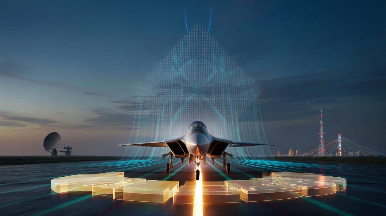
For two decades, the true limit on advanced radar systems has not been stealth aircraft or jamming, but excess heat trapped inside their chips. A Chinese research team now claims a fix that could push those limits back, with direct consequences for the military balance and future 6G networks.
Heat, not stealth, has been capping radar performance
Modern military radars increasingly rely on gallium nitride (GaN), a semiconductor that can handle much higher voltages and power densities than older gallium arsenide devices. GaN allows fighter jets, air‑defence batteries and imaging satellites to pack more power into smaller, lighter antennas.
Yet this strength brings a built‑in weakness. As power rises, GaN chips heat up fast. The hotter they get, the more engineers are forced to throttle power to avoid damage. Range, resolution and response time all suffer.
The problem becomes brutal in the X and Ka bands, the frequencies used for long‑range tracking, fire control and many satellite communications links. At those wavelengths, every extra decibel of power matters for spotting low‑observable targets or piercing through clutter and bad weather.
Inside the latest radars, performance is no longer defined by how much power you can generate, but by how much heat you can throw away.
China’s Xidian University says this thermal “ceiling” is exactly what its researchers have managed to raise.
The invisible layer that was choking super‑radars
The breakthrough does not come from a new chip architecture, exotic antenna design or clever software. It comes from a layer just a few nanometres thick, hidden deep inside the device.
In a typical GaN radar chip, different semiconductor materials are bonded together in a stack. Between them lies an ultra‑thin interface, often made from aluminium nitride. That interface is supposed to conduct heat down into the substrate, away from the active region where power is generated.
In practice, this layer behaves badly. As it grows, it tends to form tiny, disordered “islands”, riddled with irregularities. Those microscopic defects scatter heat, rather than passing it through smoothly. Over time, thermal resistance creeps up, and the chip hits a hard limit on safe operating power.
➡️ Nutritious and functional, sweet potato goes beyond the traditional plate
➡️ Gardeners who change planting order reduce competition stress
➡️ If you feel unsettled when routines change, psychology explains the need for stability
➡️ Scientists observe a rapid destabilization of polar air masses affecting mid-latitude climates
The team led by researcher Zhou Hong focused exactly on this bottleneck. By re‑engineering how that interface grows, they forced it to form a smoother, more continuous layer, like polishing a clogged pipe into a clean conduit.
Xidian University reports a cut of roughly one‑third in thermal resistance inside GaN power devices, simply by reshaping the buried interface layer.
The impact on performance, according to the published data, is striking: radar power output up by about 40 percent without changing chip size or overall energy consumption.
What a 40 percent power boost really means on the battlefield
A 40 percent gain in usable power may sound modest on paper. On radar screens, it changes tactics.
- Detection range increases without enlarging the antenna.
- Target discrimination improves at long distance, helping pick drones or cruise missiles out of clutter.
- Resistance to jamming grows, as the radar can push a stronger, cleaner signal.
- Refresh rates can climb, giving faster tracks on manoeuvring or hypersonic threats.
For a stealth aircraft, that translates into seeing earlier while emitting less often, maintaining a low signature. For a ground‑based air‑defence radar, the same hardware can cover more sky or watch one sector with finer detail. For truck‑mounted systems, it means better performance without heavy liquid‑cooling kits or large generators.
Zhou emphasises another constraint: physical size. Fighter radars live inside cramped noses and must share space with infrared sensors, datalinks and weapons computers. Gaining range and resolution without enlarging the chip is gold for aircraft designers.
China’s industrial edge: from gallium mines to warplanes
This research does not emerge in a vacuum. China is already the dominant producer of gallium, the metal at the heart of GaN technology. In recent years, Beijing has tightened export controls on gallium products, with a clear eye on military use in the US and allied countries.
That control over raw materials feeds into a broader push around so‑called “third‑generation” semiconductors such as GaN and silicon carbide. These materials tolerate high voltages and high temperatures far better than standard silicon, making them ideal for radars, power electronics and electric vehicles.
Beijing now sees GaN and its successors as a strategic technology stack: from the mine and chemical plant, through epitaxy and chip making, all the way to fighters and satellites.
Xidian University frames its work as a step toward “fourth‑generation” materials like gallium oxide, which promise even wider bandgaps and higher breakdown voltages. If such materials can be integrated with the new thermal interface techniques, future radar chips could run hotter, longer and at higher frequencies than today’s systems.
Where this thermal fix will show up first
The clearest early users are likely to be Chinese military platforms already designed around GaN active electronically scanned array (AESA) radars, such as the J‑20 and J‑35 fighters or long‑range air‑defence systems.
But the same type of high‑power GaN amplifiers also sits inside civilian and dual‑use infrastructure:
- Ka‑band satellite communication links, for broadband internet and secure military relay.
- 5G base stations pushing high‑throughput beams into dense urban areas.
- Experimental 6G testbeds, which target even higher frequencies and data rates.
In December, another team at Xidian presented a radar‑like device that converts ambient electromagnetic waves into usable electricity, a sign that Chinese laboratories are attacking radio‑frequency challenges from multiple angles.
How the new approach changes performance‑vs‑cooling trade‑offs
Traditionally, engineers balance radar performance against cooling weight and complexity. Extra power means more coolant loops, pumps, heat exchangers and maintenance. That adds weight to aircraft and takes up valuable space on satellites and ships.
By reducing thermal resistance inside the chip itself, the new Chinese method alters that balance. The same coolant system can now support a more powerful radar. Or designers can keep performance steady, shrink the cooling hardware and free up mass for fuel or payloads.
| Design choice | Old trade‑off | With improved thermal layer |
|---|---|---|
| Boost radar power | Needs bigger cooling, more weight | Some gains possible with no extra cooling |
| Keep power constant | Standard cooling hardware | Option to shrink cooling and save weight |
| Run at high duty cycle | Risk of rapid overheating | Safer continuous or burst operation |
Civil networks could benefit too. Improved heat extraction allows telecom operators to run GaN amplifiers more efficiently, potentially covering wider areas with the same number of towers, or cutting energy bills in data‑hungry zones.
Key technical terms worth unpacking
What “ultrawide bandgap” actually means
The Xidian study, published under the title “Heterogeneous integration of ultrawide bandgap semiconductors for radio frequency power devices”, centres on materials with very wide bandgaps. In semiconductor physics, the bandgap is the energy gap between electron states inside a crystal.
A wider bandgap lets a material withstand higher voltages and temperatures before it breaks down. GaN and gallium oxide fall into this category, which is why they are so attractive for power electronics and radars. The challenge lies in stitching together different crystals without creating thermal dead zones.
Why thermal resistance matters as much as electrical resistance
Engineers pay as much attention to thermal resistance as they do to electrical resistance. Electrical resistance wastes energy as heat; thermal resistance then determines how fast that heat can escape. High thermal resistance means heat piles up where it is least welcome.
By smoothing the interface layer between GaN and the substrate, the Xidian team has essentially lowered the “thermal ohms” inside the chip. The same current now raises the temperature less, or, put differently, the chip can carry more current before hitting its thermal limit.
Risks, benefits and future scenarios
The benefits for China are straightforward: longer‑range, finer‑resolution radars that sit on top of an already strong supply chain for gallium and GaN devices. That may sharpen debates in Washington, Tokyo and Brussels about export controls and domestic investment in competing technologies.
There are risks too. Lower thermal constraints encourage designers to push power levels higher. That could create an arms race in high‑power radio‑frequency emissions, raising questions about electromagnetic interference, safety around dense civilian networks, and the vulnerability of electronics to harsher RF environments.
One plausible scenario over the next decade is a layered effect. Improved GaN devices first upgrade existing radars, giving better coverage and tracking. In parallel, telecoms use the same thermal advances to roll out more capable 6G‑ready infrastructure. Combined, these shifts may tighten the integration between military and civilian networks, where high‑resolution sensing and high‑capacity communications share common hardware roots.
For now, the message is clear: by solving a hidden heat bottleneck inside GaN chips, Chinese researchers have taken a quiet but meaningful step toward dominating the next generation of “super‑radars” and the communications systems that feed them.